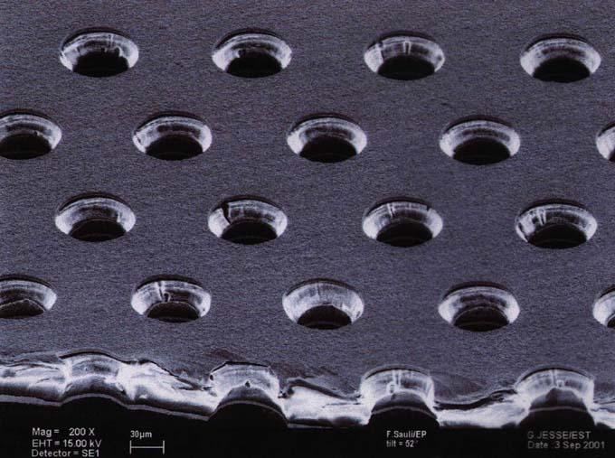
Previous methods to produce microvias are based on complex technologies such as laser, plasma or photo imaging. Chemical Via is a new chemical method to make microvias for high density printed multilayer circuits. Microvias are used to interconnect adjacent layers and consist of a small diameter hole (usually 70µm) with a thin metallic deposit covering their cylindrical walls to ensure the local conductivity between the bottom and top layers. Microvias of any shapes and dimensions are made possible at a low production costs. The technology was used by CERN PCB manufacturing workshop for the production of PCboards for HEP needs.
Advantages & Applications
Applications
- Microelectronics
- PCBs industry
Advantages
- Vias of several possible dimensions from microns to centimeters
- Initial fabrication investment to use method is low
- Vias of any shape (circle, star, square, etc) can be produced and standardized
- Process or method compatible with all standard PC assembly lines
Specifications
Specifications
- Etching time (9-18 min)
- An isotropic Etching technique (Deep reactive ion etching) is used
- Minimum via diameter (40µm)
Innovative features
- Easy elimination of elements (e.g. glue) by dissolving using a chemical process.
- Kapton carving by using a sequence of simple chemical baths.
Patents
Description
Patent: WO03055288.
Licensing
Ready for licensing. Patented technology, WO03055288.